Castellated Holes in PCB Design
- Lentark Electronics

- Jan 2, 2021
- 2 min read

Castellated holes are used to mount one PCB onto the surface of another PCB or to create custom edge-connection structures on a circuit board. They can be designed in different forms depending on the application.
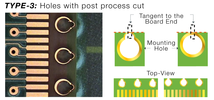
In many cases, they appear as half-plated holes along the edge of the PCB. However, depending on the manufacturing method and design requirement, they may also look like a smaller or larger section of a cut circular hole. This structure can help with alignment during soldering and provide a practical mounting surface between boards.
Similar to mounting SMD components onto a PCB surface, castellated holes allow one PCB to be soldered directly onto another PCB. To achieve this, plated holes are placed along the PCB edge and then cut or routed according to the design. After this process, properly plated and clean mounting surfaces are formed on the board edge.
Why Are Castellated Holes Used?
If you have circuit blocks that are used repeatedly in similar applications, such as small inverter circuits, filter circuits, wireless modules or other reusable design sections, these circuits can be placed on a separate PCB and designed with castellated holes on the edges.
This approach can provide several practical advantages:
The circuit can be produced as a small module.
In case of a fault, the module can be removed from the main board and tested separately.
The same module can be reused in similar applications.
The module can be mounted either by pin connection or surface mounting, depending on the design.
Castellated Hole Design Variations
Castellated holes can be designed in different shapes and dimensions depending on the PCB thickness, manufacturing process, soldering method and mechanical requirements of the application.


In some designs, the hole is divided almost exactly in half. In other designs, only a smaller section of the hole remains on the board edge. The final geometry should be selected according to both electrical connection requirements and manufacturing limitations.
Recommended Design Features for Castellated Holes
Hole size: The hole diameter should be selected as large as possible within the limits of the design. Larger holes generally make the plating and soldering process easier.
Pad size: The pad area should be kept as wide as possible on both the top and bottom layers of the PCB. A larger pad area can improve solderability and mechanical strength.
Surface finish: The surface finish depends on the application and manufacturing preference. However, ENIG finish is often preferred because it can make the process easier and provide a clean solderable surface.
Number of holes: The number of castellated holes depends on the circuit and mechanical requirements. However, an optimum number should be selected. Using too many holes may make alignment and assembly more difficult.
Conclusion
Castellated holes are a practical design option when a circuit block needs to be used as a small module or mounted directly onto another PCB. With proper hole size, pad design, surface finish and manufacturing control, they can provide both electrical connection and mechanical support in compact electronic designs.


Comments